What is the bevel scan?
Bevel scan is VPD solution scan the edge of wafer 1 to 5 mm to collect the metal of wafer edge (include wafer surface and backside.
Why Bevel scan needed?
Reason is:
1. To verify if the cassette is clean, as wafer edge always touch the cassette, if the cassette is dirty, it will contaminate wafer.
2. To verity if the robot of process system is clean which used edge-gripper robot. If the robot is dirty, it will contaminate wafer.
3. Any tool or system which will contact the wafer edge during the IC making process much be monitor the bevel contamination of wafer
How Bevel scan execute and collect the metal?
Step 1. Load wafer to Pad fume, and do fume process with 49% HF
N2 flow into bottle which filled with 49% HF, and HF evaporate into fume chamber. HF and SiO2 chemical reaction as follow:
6 HF + SiO2 à H2SiF6 + 2 H2O
After this chemical reaction, wafer surface and bevel become hydrophobic
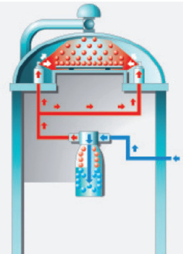
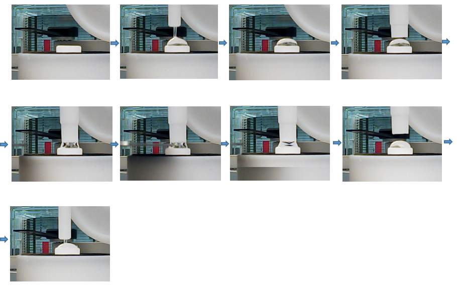
Step 2. Load wafer to Pad scan module:
After wafer alignment, scan tube, pipette tube cleaned, VPD solution was dropped on droplet holder. Then the scan tube catches the VPD solution to form a column of solution, then wafer edge goes into the solution, and wafer stage rotate. VPD will collect the metal of wafer edge during the stage rotation. After the scan, Pipette will transfer the VPD solution into a clean vial, then measure the contamination by ICPMS.
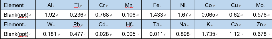
 VPD system Bevel scan module blank test data:
Requirement:
ICPMS: Agilent 8900
Chemical: TAMA pure Acid, metal contamination<10ppt
Wafer size: 300mm
Bevel Scan Blank: