MFM-3000F Wafer Thickness No-contact Measurement Equipment
Work Principle:
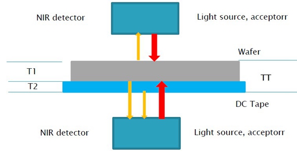
The device is equipped with two upper and lower NIR detectors, which obtain the TT thickness by obtaining the position of the detector and the reflection of the silicon chip, and then obtain the DC tape thickness T2 by penetrating the DC tape through NIR, thus obtaining the data of the silicon chip thickness T1.
Technology Parameters:
NIR image location thickness measurement module (Wave legnth 840um)
-
Maximum Range: 1000um
-
Minimum signal layer measured thickness: 10um
-
Minimum signal layer Resolution: 0.35um
-
Display Resolution: 0.0um
-
Signal layer measured repeated accuracy
-
(Point repetition accuracy of a single point with linear error of thickness ) Signal layer thickness > 50 um: < ± 0.01 x measurement monolayer thickness <= 50 um: ± 0.5 um
-
(Point repetition accuracy of single point measure without linear error of thickness) 20±1 degree C, repetition accuracy < ± 0.5um
-
When the ambient temperature and vibration are more stable, the roughness of the measured sample reaches Rz<0.1um, and the repetition precision reaches ± 0.1um
Upper superthin film measurement module
-
Measured Location Size: 40um
-
Maximum film measured thickness: 50um
-
Minimum film measured thickness: 1um
-
Minimum Display resolution: 0.01um
-
Repeated measured accuracy: ± 0.25 um
-
High resolution visible optical spectrometer
Equipment can add white light interference objective to reach 3D scanning and measurement.